TEMPORARY PROCESS PROTECTION
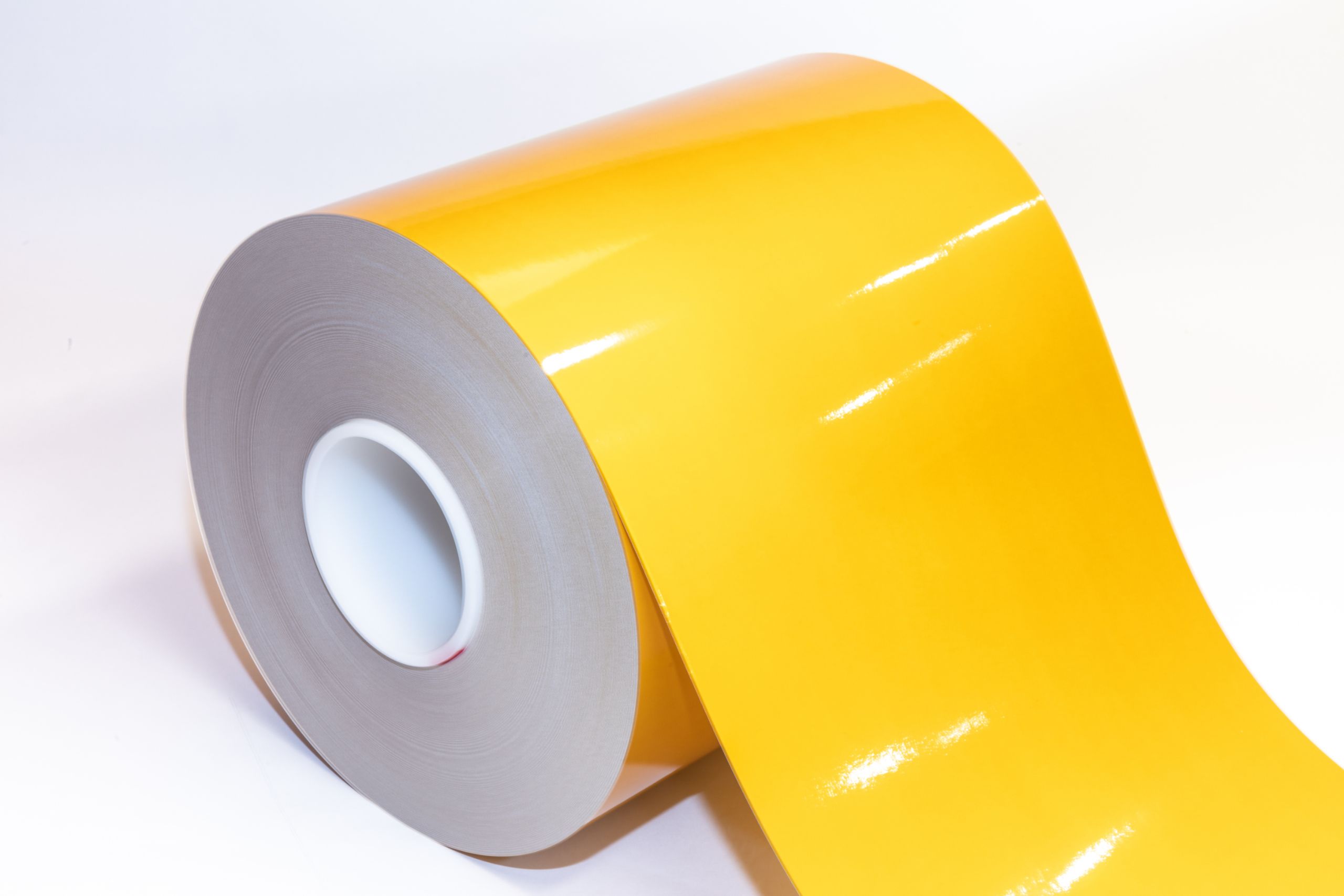
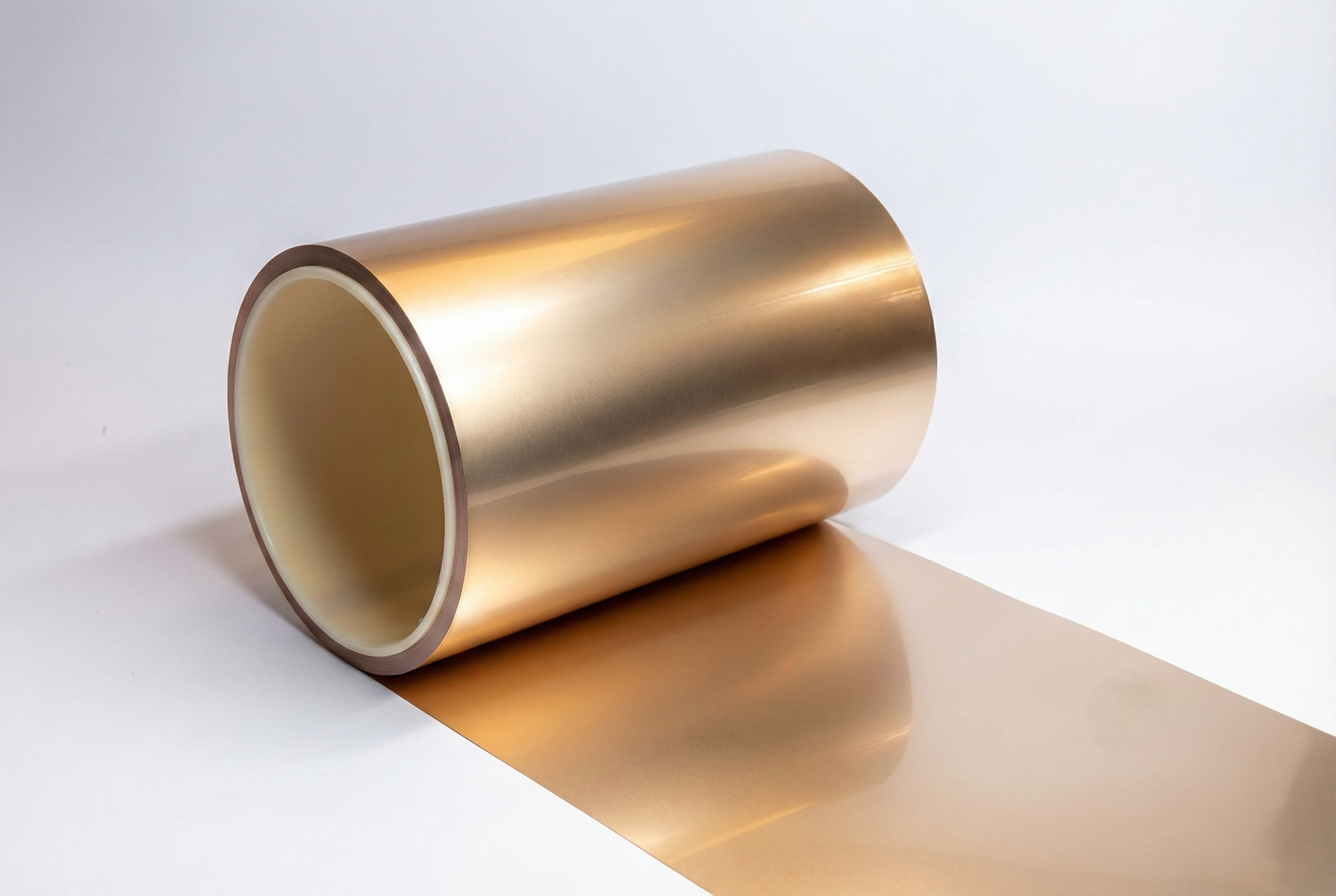
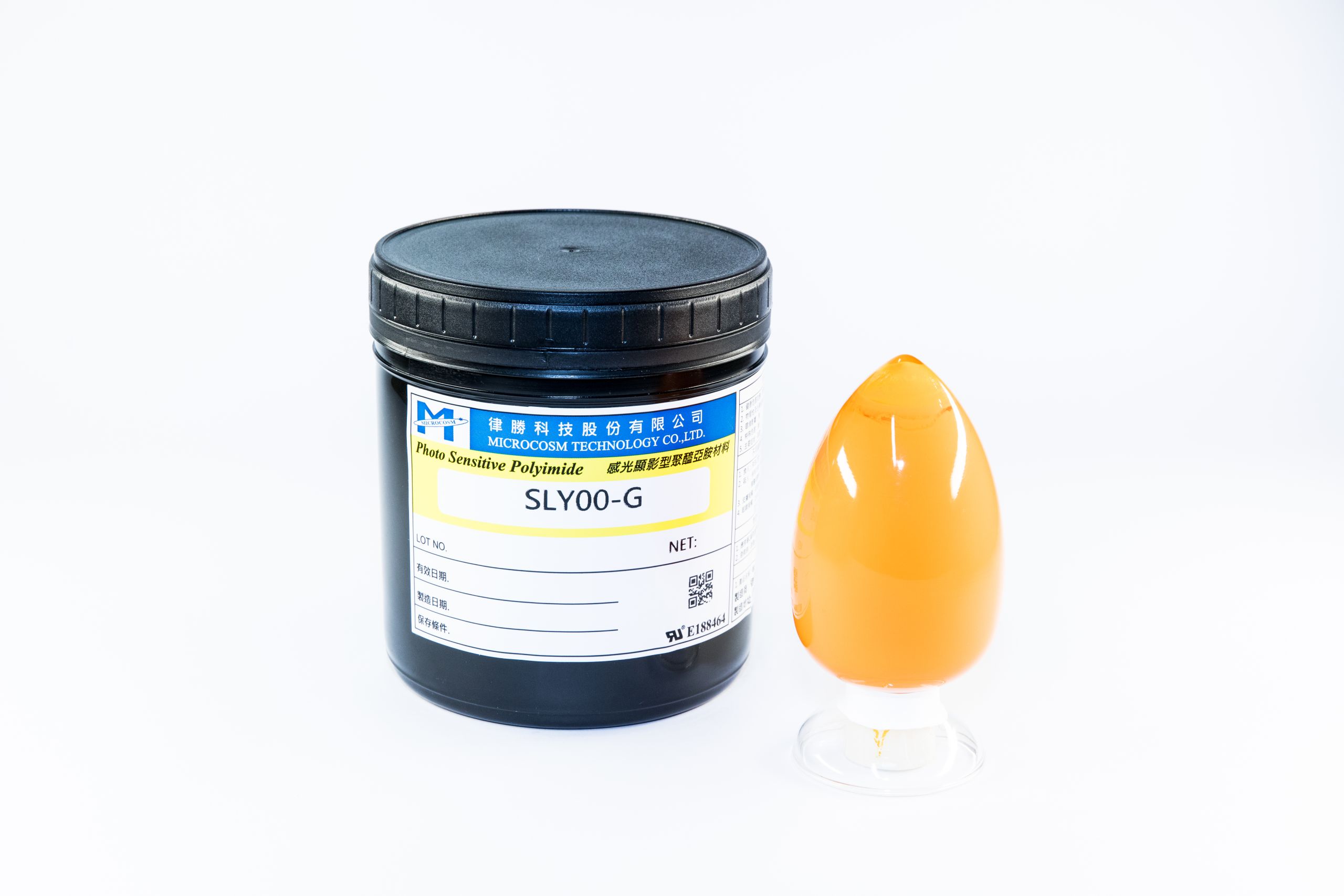
Photosensitive High-Temperature Peelable PSPI
A photosensitive high-temperature temporary protection material for PCB, substrates, and advanced semiconductor packaging processes. Selective protection and opening areas can be defined through exposure and development, withstand subsequent high-temperature and lamination processes, and be removed by alkaline stripping after processing.
A photosensitive high-temperature temporary protection material for PCB, substrates, and advanced semiconductor packaging processes. It enables selective protection, withstands high-temperature and lamination processes, and can be removed by alkaline stripping after processing.
Material Overview
Selective Temporary Protection for Precision Electronic Processes
Photosensitive peelable PSPI is designed for areas requiring local temporary protection in PCB, substrate, and advanced semiconductor packaging processes. The protection area can be defined according to product structure and process requirements, providing temporary protection for subsequent high-temperature, lamination, and machining processes.
Confirmed Performance
Core Performance of Photosensitive Peelable PSPI
Crack-Free High-Temperature Processing
Designed for stable temporary protection during high-temperature baking, lamination, and related process conditions.
Film Thickness Range
Supports different step heights and protection requirements with a broad process adjustment window.
Clean Alkaline Removal
Representative stripping conditions: after baking at 200°C, 4% NaOH at 50°C for 3–5 min. Actual conditions may be adjusted according to material grade, film thickness, and process requirements.
Imaging Resolution
Supports local window openings and defined protection patterns for fine-area process evaluation.
Application Paths
Explore Processes by Application
The material provides the same core performance, while structures, patterns, and downstream processes are presented separately for PCB and advanced semiconductor packaging applications.
APPLICATION 01 — PCB
High-Temperature Temporary Protection in PCB Processes
Provides local temporary protection and resin-flow blocking for cavities and recesses, step structures and gold fingers, PP/AD window openings, optical modules, and related processes.
Why Is Peelable PSPI Needed in High-Temperature PCB Processes?
Temporary Protection During High-Temperature Lamination
Protects designated areas during high-temperature, lamination, and downstream machining processes while maintaining an intact, crack-free protection layer.
Resin-Flow Blocking for Cavities and Recesses
Provides temporary protection for cavities, recesses, and local openings, helping block resin flow and reduce the risk of PP/AD intrusion, residue, or contamination of downstream machining areas.
One-Step Definition of Fine Patterns
Exposure and development define multiple selective protection and opening areas in one process, making it more suitable for complex patterns and multi-area processing than individually applied, cut, and aligned tapes.
Effective Low-Residue Removal After Processing
After downstream processing, the protection layer is removed by alkaline stripping to reduce film residue and subsequent cleaning requirements while supporting process stability and yield.
How Is Photosensitive Peelable PSPI Used in PCB Processes?
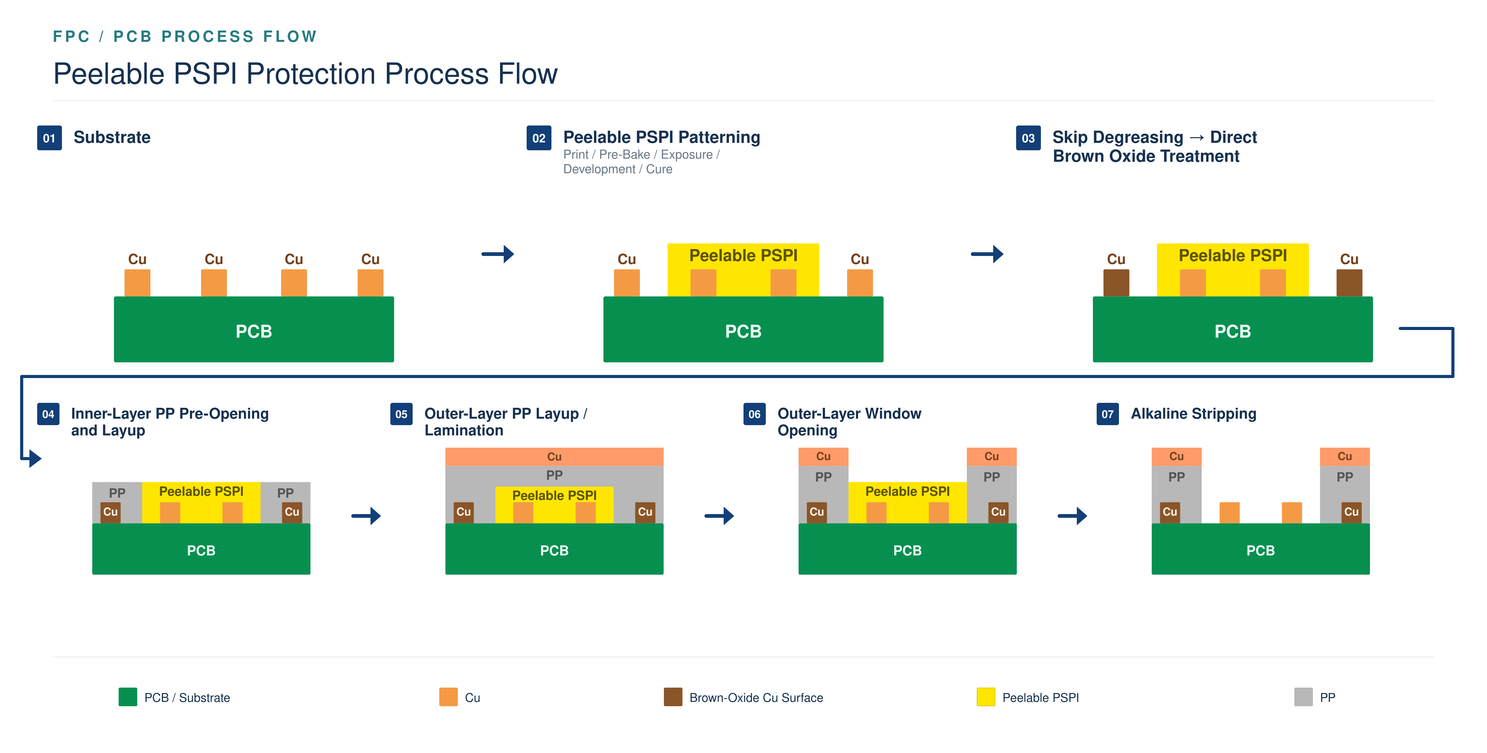
Swipe right to view the full process →

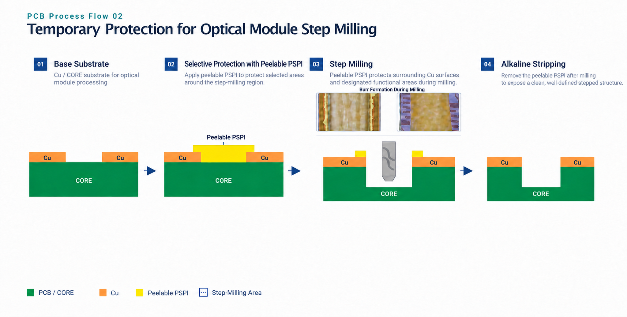
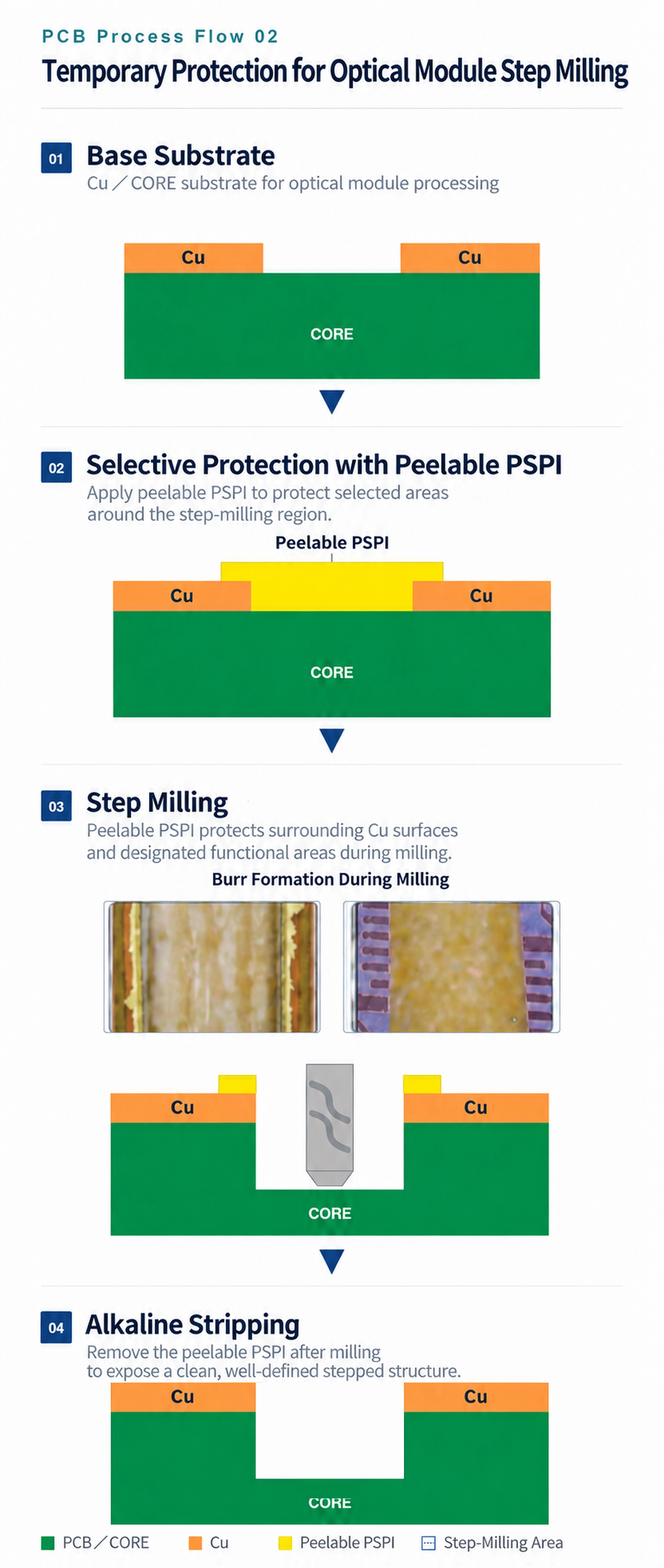
PCB Process Flow 02
Temporary Protection for Optical Module Step Milling
Primary PCB Applications
Depending on the PCB structure and process requirements, the material can provide local protection for cavities, step structures, gold fingers, resin-flow blocking at window openings, and machining-burr protection.
PCB Rigid Board: Temporary Protection for Cavity and Recess Structures
Designed for PCBs with cavities, local recesses, or embedded structures. Peelable PSPI temporarily protects designated areas during lamination and downstream machining, reducing the risk of PP/AD intrusion, residue, or process contamination.
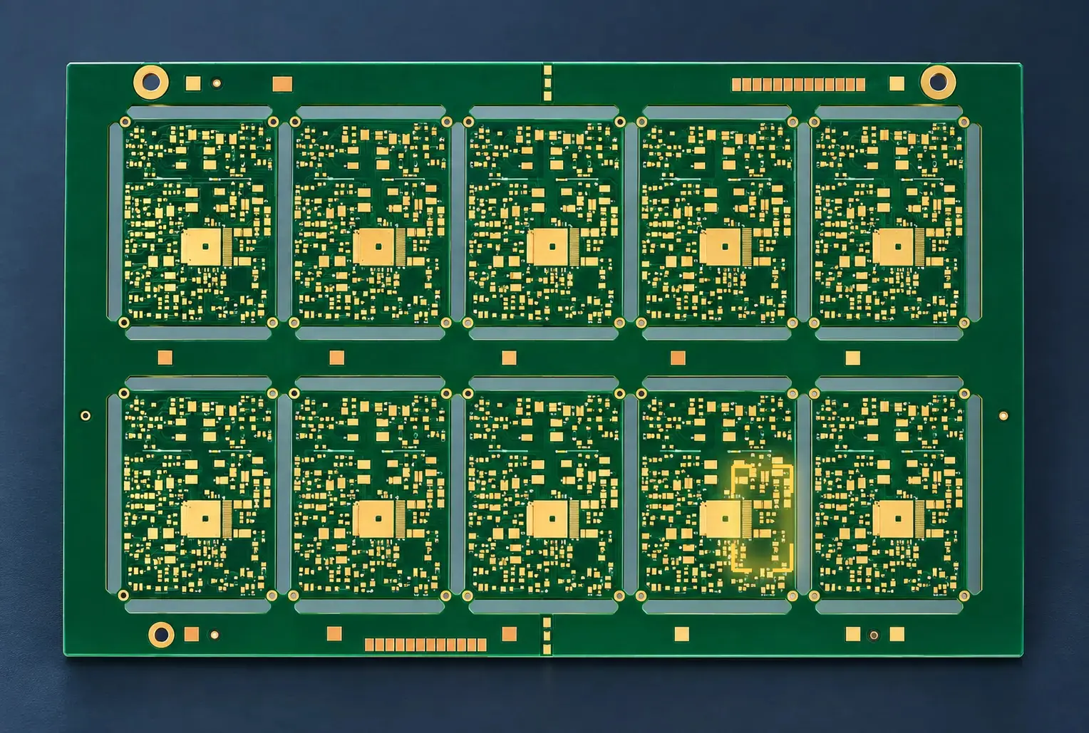
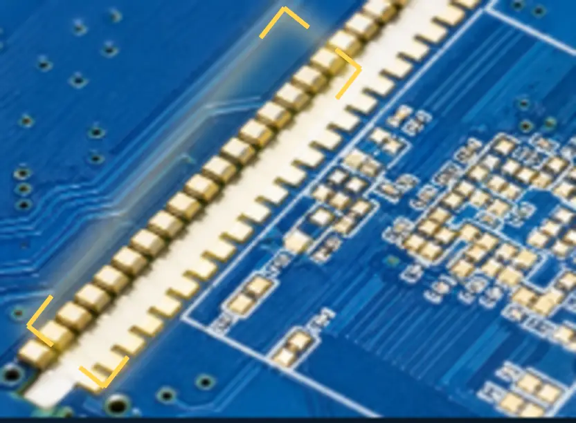
FPC/Rigid-Flex: Temporary Protection for Step Structures and Gold Fingers
Suitable for step structures, gold fingers, rigid-flex transition areas, local openings, and machining-burr protection. Photosensitive patterning can define multiple protection areas in one process, reducing the risk of resin, debris, or machining contamination in designated functional regions during lamination or downstream processing.
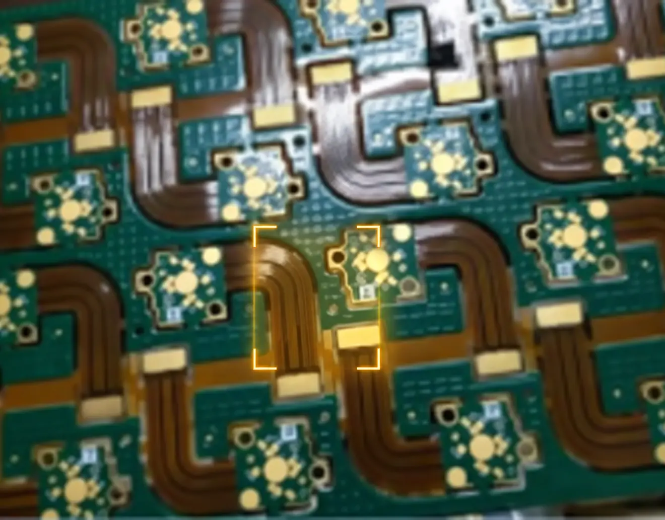
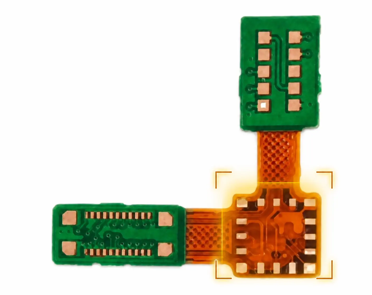
APPLICATION 02 — SEMICONDUCTOR
Temporary Cavity Protection in Advanced Packaging Processes
In cavity and recess structures and multi-chip interconnect packaging processes, peelable PSPI is applied to designated areas before build-up layer lamination, circuit patterning, and cavity opening. After completing its protection function, it is dissolved and removed under the recommended alkaline conditions for subsequent silicon bridge or μ-bump embedding and assembly.
Cavity Opening Structure Process Protection Flow
Swipe right to view the full process →
Substrate
Peelable PSPI Coating
Build-Up Material Lamination
Circuit Patterning / Cavity Opening
Alkaline Removal of Peelable PSPI
Silicon Bridge / μ-Bump Embedding
Copper
Peelable PSPI
Build-Up Material / ABF
Si Bridge / PIC
Interconnect Structure
Advanced Packaging Application Scenarios
CPO Packaging Application
In a CPO (Co-Packaged Optics) structure, the ASIC and EIC are located on the package substrate surface and connected by circuit interconnects. The PIC is embedded in a cavity beneath the EIC to form the EIC–PIC interconnect. Peelable PSPI provides temporary protection for designated areas during cavity formation and build-up lamination.
AI Multi-Chip Packaging Application
HBM, SoC, and ASIC are located on the package substrate surface. Two embedded silicon bridges span the HBM–SoC and SoC–ASIC chip boundaries to form high-density, short-distance interconnects. Peelable PSPI provides temporary protection for designated structures and processing areas during Si Bridge cavity formation and downstream processes.
Technical Data
Representative Technical Data
The following data are representative test results. Actual product specifications and recommended process conditions should be confirmed according to the product grade and application conditions.
| Test Item | Test Condition | Unit | Representative Value |
|---|---|---|---|
| Film Thickness | Screen Printing / Dispensing | μm | 20–300 |
| Exposure | Wavelength: 365 / 385 / 405 nm | mJ/cm² | 200–500 |
| Development | 1% potassium carbonate (K₂CO₃) or sodium carbonate (Na₂CO₃), 30°C | sec | 60–120 |
| Resolution | Round Hole / Line Width | μm | 100 |
| Stripping | 4.0% NaOH, 50°C (film thickness: 25 μm; curing condition: 200°C × 2 hr) | min | 3–5 |
Frequently Asked Questions
Frequently Asked Technical Questions About Photosensitive Peelable PSPI
What Is Photosensitive Peelable PSPI?
Photosensitive peelable PSPI is a photosensitive temporary protection material for precision electronic processes such as PCB, substrates, and advanced semiconductor packaging. Exposure and development define designated selective protection and opening areas. The material provides local protection during subsequent high-temperature, lamination, or machining processes and is removed by alkaline stripping after processing.
What Are the Key Features of Photosensitive Peelable PSPI?
Photosensitive peelable PSPI combines photosensitive patterning, resistance to high-temperature and lamination processes, and alkaline stripping after processing. It can form designated selective protection and opening areas according to the design and is suitable for cavities and recesses, step structures, gold fingers, resin-flow blocking at window openings, and other local temporary protection processes.
How Does Photosensitive Peelable PSPI Form Selective Protection Areas?
PSPI is first coated uniformly on the substrate surface, then patterned through photomask exposure and development to form local protection patterns.
This allows selective protection areas to be formed at cavities, local recesses, step structures, gold fingers, or other designated locations according to the product design, without manually cutting tape to create complex patterns.
Pattern dimensions and resolution can be optimized according to film thickness, exposure equipment, photomask design, and actual process requirements.
Can PSPI Still Be Cleanly Removed After High-Temperature or Lamination Processes?
Yes. A typical lamination condition is 230°C, and the material can also accommodate higher-temperature processes. The applicable range can be evaluated according to process conditions such as temperature, pressure, time, and film thickness. After high-temperature or lamination processing, the protection layer can still be removed by alkaline stripping.
How Is Photosensitive Peelable PSPI Removed After Processing?
After processing, PSPI can be dissolved and removed through an alkaline stripping process.
The material is compatible with alkaline stripping equipment and process conditions commonly used by PCB and FPC manufacturers.
Representative test conditions include:
- 4% sodium hydroxide (NaOH)
- 50°C
- approximately 3–5 minutes
for complete removal.
These are representative process conditions rather than fixed requirements. The alkaline solution type, concentration, temperature, and treatment time can be adjusted according to the customer’s existing production line, film thickness, and prior thermal history.
In addition to sodium hydroxide (NaOH), potassium hydroxide (KOH) or other alkaline removal systems may be evaluated according to process requirements.
Microcosm can recommend suitable stripping parameters based on the customer’s existing stripping line and process conditions.
How Is Photosensitive Peelable PSPI Different from Conventional PI Protection Tape?
PI protection tape typically forms protection areas through application, cutting, or die cutting. Photosensitive peelable PSPI uses exposure and development to form multiple designated selective protection and opening areas in one process. For cavities and recesses, step structures, gold fingers, or multiple local protection locations, it reduces individual tape application, cutting, and alignment operations. After processing, PSPI is removed by alkaline stripping, whereas PI tape is typically removed by physical peeling.
Which PCB Processes Are Suitable for Photosensitive Peelable PSPI?
Photosensitive peelable PSPI can be used in various PCB temporary protection processes, including:
- Temporary protection of cavity and recess structures
- Protection of step structures, gold fingers, and local areas
- PP/AD resin-flow blocking at window openings
- Selective protection during multi-material stacking and lamination
- Local protection for optical-module-related processes
- Protection against cutting or machining burrs
- Processes requiring protection-layer removal after high-temperature processing
Material and process matching can be further evaluated for different substrate materials, film thicknesses, pattern dimensions, and downstream process conditions.
What Is a PCB Cavity?
A PCB cavity is a local recess or hollow region formed in a circuit board or package substrate. It can accommodate chips or embedded components or create a localized step structure.
Peelable PSPI can define cavity or recess locations requiring temporary protection. After lamination, machining, or high-temperature steps, it is dissolved and removed under the recommended alkaline conditions.
Can Photosensitive Peelable PSPI Be Used for Cavity or PP/AD Window Opening?
Yes.
Photosensitive peelable PSPI can be used for temporary protection of cavity and recess structures and PP/AD resin-flow blocking at window openings.
Because the material forms designated patterns through exposure and development, it can precisely define patterns according to window locations and protection areas. Compared with manually applied and cut tape, it is more suitable for protection requirements involving multiple areas, complex shapes, or high-accuracy alignment.
For evaluation, provide conditions such as cavity depth, window dimensions, target film thickness, lamination temperature, pressure, and time. Microcosm can assist with process setup.
Can Photosensitive Peelable PSPI Be Used in Semiconductor, Substrate, or Package-Substrate Processes?
Yes.
Photosensitive peelable PSPI can be used for selective temporary protection in semiconductor, substrate, and package-substrate processes.
The material forms designated protection areas through exposure and development and provides local protection during subsequent high-temperature, lamination, or multi-material stacking processes. After processing, the protection layer is removed with an alkaline stripping solution.
It is therefore suitable for processes requiring:
- Fine-pattern protection
- Local Window Opening
- Selective protection of multiple areas
- Removal after high-temperature or lamination processing
- Integration with existing wet processes
in semiconductor, substrate, and package-substrate applications.
Microcosm can recommend suitable materials and process conditions based on the substrate structure, film thickness, thermal history, and downstream processes.
What Process Information Is Required for Evaluation?
To support efficient material and process matching, please provide:
- Application and substrate type
- Protection location and structure
- Window / protection-area dimensions
- Target film thickness
- Maximum process temperature
- Lamination pressure and time
- Subsequent chemical or machining processes
- Intended PSPI removal stage
- Existing stripping equipment and alkaline conditions
Microcosm can recommend material selection, process settings, and stripping conditions based on this information to support integration into the customer’s existing process.
Process Evaluation
Evaluating a High-Temperature Temporary Protection or Photosensitive Peelable PSPI Process?
Please provide your key process conditions so our technical team can evaluate the appropriate material and recommended process conditions based on your actual structure and application requirements.
- Application / Substrate Type
- Process Temperature
- Target film thickness
- Window / Protection Dimensions
- Downstream Process Conditions
Technical Evaluation Process
Evaluation Process After Submitting Your Requirements
From confirming process conditions and selecting materials to recommending an evaluation direction, our team supports preliminary material and process assessment.
Submit Process Requirements
Provide key conditions such as the application, substrate, process temperature, film thickness, and protection dimensions.
Confirm Application Conditions
Confirm the material and test conditions according to the structure, pattern, and downstream processes.
Provide Evaluation Direction
Recommend a suitable product and follow-up test direction for engineering validation and discussion.