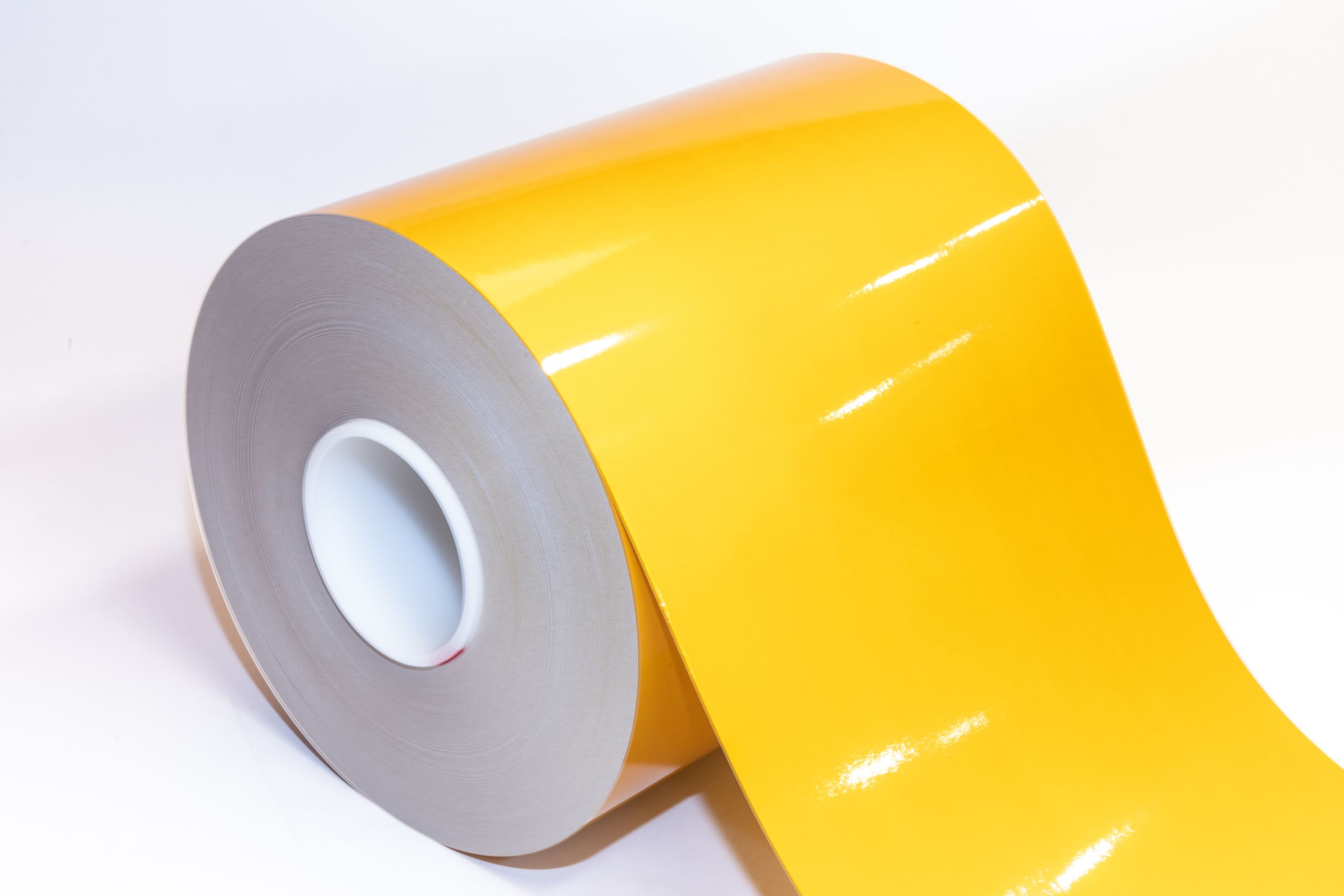
Zero-Residue Protective Adhesive Designed for Open-Cover Processes
Photosensitive High-Temperature Peelable PI is a high-performance protection material specifically developed for cavity step openings, through-hole protection, optical module burr suppression, and PP/AD window blocking processes.
It features high-resolution image patterning, no cracking at process temperatures up to 230°C, clean alkaline peeling with no residue, and controllable step-filling capability.
The material supports screen-print thicknesses from 20 to 150 μm, adapting to a wide range of processing requirements. It is non-reactive with PP substrates and can be completely removed, significantly improving process stability and manufacturing yield.
Common Challenges and Limitations
In precision PCB fabrication, cavity structures, 3D stepped boards, optical modules, and substrate manufacturing, do you often encounter the following issues?
- Protective films (peelable coatings or PI tapes) crack or leave residue after high-temperature lamination, requiring rework
- Residual adhesive after peeling is difficult to remove, affecting downstream processes and long-term reliability
- Irregular blocking edges and excessive burr formation lead to yield loss
- Small pad openings combined with excessive PP/AD resin flow make adhesive control difficult
- Fine-line areas require high resolution while overall thickness must be reduced, but conventional materials cannot meet both needs
- Excessive rebound force in bending modules negatively impacts overall assembly
- Poor planarization control in multilayer cavity structures with large step heights
Microcosm’s Photosensitive High-Temperature Peelable PI provides a complete solution to the challenges listed above.
Product Advantages
| Feature | Description | Product Values |
|---|---|---|
| Screen-print thickness | 20–150 μm | Wide thickness adaptability improves process flexibility and surface planarization |
| Pre-bake temperature | 75–90°C | Lower processing temperature improves substrate safety |
| Imaging resolution | 100 μm | High imaging precision ensures clean and well-defined small openings |
| High-temperature resistance | 230°C without cracking | No cracking risk during high-temperature baking or reflow |
| Peeling time | 3–5 mins (NaOH 4% 50°C ) | Clean removal without substrate damage or residue |
Why Choose Us?
See the Product Comparison
| Performance Metric | Microcosm Photosensitive High-Temperature Peelable PI | Standard Peelable Materials |
|---|---|---|
| High-temperature resistance | ★★★★☆(No cracking at 230°C ) | ★★☆☆☆ (Prone to cracking) |
| Residue control | ★★★★★ (Residue-free) | ★★☆☆☆(Residual adhesive) |
| Imaging resolution | ★★★★★(Stable fine-area patterning) | ☆☆☆☆☆ (Non-photosensitive) |
| Thickness adaptability | 20-150 μm | Limited to thick films |
| PP/AD compatibility | Non-reactive, controlled resin overflow | Poor control, prone to residue |
The Optimal Solution
The SLY00-PU series outperforms comparable materials in thermal resistance, imaging precision and clean peelability, significantly improving process stability and yield. Photosensitive High-Temperature Peelable PI is the ideal solution for cavity and stepped boards (stepped gold fingers, stepped vertical power planes), optical modules, and advanced substrate manufacturing.
Product Application Structure
Process Protection Applications for Cavity Step / Stepped Gold Finger Structures
 (2)")
- Burr Protection Applications for Optical Modules

PP/AD Window Opening Solder Mask Blocking Applications